I’ve managed (at least I think I did since it produced the proper output as the table in the PDF of project 4) to design stack(n) (n=8 in our case) with exactly n registers/flip-flops, 2 gates, 1 inverter and a single 2:1 mux. Is this of any relevance to part 1 of the assignment? Or do I have to make a design that somehow exactly fit to the figure in the file, even if it is less efficient with many more mux’s and FF’s/registers?
I doubt it if your circuit has just 2 gates in total…
I want to emphasize what the question is about.
The question is about how to design a stack in hardware such that:
- all nets have constant fanout
- the longest combinational path is bounded by a constant (regardless of the stack size)
- the circuit is build from copies of the same module (that happens to be an FSM) with flip-flop along the wires connecting neighboring modules.
I was referring to the regular “stack” (the first one, not the later ones). I realize now that even though it works its probally not what was asked for. Anyways, here is what it looks like:
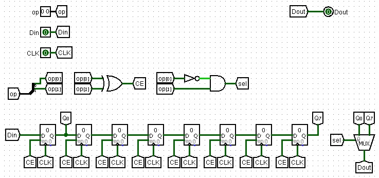
This looks like a one directional shift register.
Why do you think it has anything to do with a stack?
It’s similar but it’s not exactly a one directional shift register because of the condition on the output and CE. A stack is some form of a bi-directional shift-register, no? And this one did manage to produce exactly the correct result (not just push, but also pop as well) as appeared in the table of the PDF file.
However, for the purpose of doing the other parts I already came up with a different design and abandoned this one.